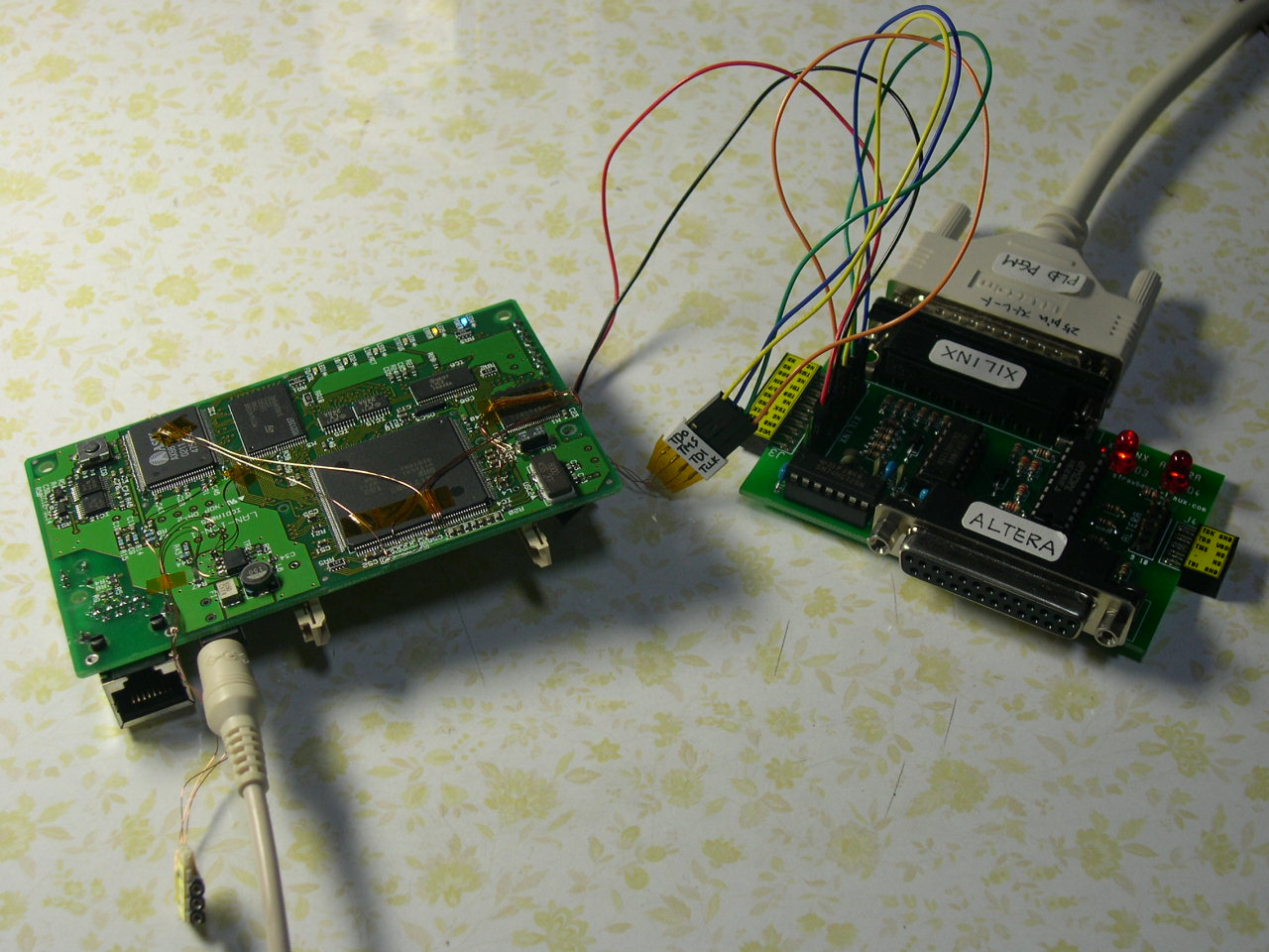
JTAG プログラミングケーブルを使って、 SH3(SH7709S)のバスにつながっているFLASHをプログラミングします。 FLASHをプログラムする程度ならば、CPU デバッガは不要です。
JTAGの基本的な4つの信号線(TDI,TDO,TCK,TMS)をつなぎます。 プログラミングケーブルはターゲットからの電源供給を必要とするので、 3.3V(H-UDIコネクタにはありません)を見つけてつなげます。 よって、GNDも含めて計6本のワイヤリングをします。
また、JTAGインタフェースを有効にするために、xASEMD0をLにします。 ここまでのことで、SHのピンの状態を観察することができます。
ただし、バスやIOポートを直接コントロールしたり、FLASHのプログラミングのためには CPUをスリープさせた状態を作ったほうがよいため、リセット周りの工夫が必要です。(後述)
% cd <WORKDIR>
% tar xvfj include-0.3.2.tar.bz2
% tar jtag-0.5.1.tar.bz2
% cd jtag-0.5.1
% ./configure --with-include=<WORKDIR>/include-0.3.2
% make
# make install
# cd /usr/local/share/jtag/hitachi # vi PARTS ------------ SH7709 用のエントリを追加する *** 24,26 **** --- 24,27 ---- # bits 27-12 of the Device Identification Register 0000000001000010 sh7727 SH7727 0111010101101110 sh7727 SH7727 + 0000000000000001 sh7709 SH7709 # mkdir sh7709 ------------- SH7709 用の設定ファイルディレクトリの作成 # vi STEPPINGS + 0000 sh7709 V0そして、これ(sh7709)を /usr/local/share/jtag/hitachi/sh7709 の下におきます。
% jtag
JTAG Tools 0.5.1
Copyright (C) 2002, 2003 ETC s.r.o.
JTAG Tools is free software, covered by the GNU General Public License, and you
are
welcome to change it and/or distribute copies of it under certain conditions.
There is absolutely no warranty for JTAG Tools.

Warning: JTAG Tools may damage your hardware! Type "quit" to exit!

Type "help" for help.

jtag> cable parallel 0x378 DLC5        (接続ケーブルにあわせて宣言する)
Initializing Xilinx DLC5 JTAG Parallel Cable III on parallel port at 0x378
jtag> detect
IR length: 16
Chain length: 1
Device Id: 00000000000000000001000000001111
  Manufacturer: Hitachi
  Part:         SH7709
  Stepping:     V0
  Filename:     /usr/local/share/jtag/hitachi/sh7709/sh7709
jtag>
このように出力されればCPUを認識している。
jtag> instruction SAMPLE/PRELOAD
jtag> shift ir                        (SAMPLE/PRELOAD命令を送り込む)
jtag> shift dr                        (データを転送)
jtag> dr                              (そのビット列を表示)
11111111111111111111111111111111101011111111111111111111111111111111111111111111
11111111111111111111111111111111110110010110000100000000000011111111111111110000
00000000000000000000000000000000000000111111111111111111100111111101101100000010
11001100000001101000000001110101111110111111000000011000110101000000010000000010
1111110110010000011
jtag> shift dr
jtag> dr
11111111111111111111111111111111101011111111111111111111111111111111111111111111
11111111111111111111111111111111110110010110000100000000000011111111111111110000
00000000000000000000000000000000000000111111111111111111100111111101101100000010
11001100000001101000000001110111111110111111000000011000110111100000010000000010
1111110110010000011      (CPU実行中のため微妙にビットパターンが違う)
jtag> get signal PTD1    (PTD1に接続したスイッチの状態を得る)
PTD1 = 1
jtag> shift dr           (押した状態でサンプル)
jtag> get signal PTD1
PTD1 = 0                 (状態が変わった)
信号名は /usr/local/share/jtag/hitachi/sh7709/sh7709 で定義されたシンボルが使えます。
CPUからピンを奪う場合にはCPUリセットホールド状態にする必要があります。 SH7709Sユーザーズマニュアル 22.4.2によると CPUリセット解除時に TRST が L にしておけば よいようです。ですので、リセット前(電源ON前)にTRSTをGNDにショートしておき、電源を入れ、 その後TRSTを開放することでホールド状態を作成します。
ブートローダなどがインストールされていれば、コンソールに何も表示されなくなるので、 CPUが起動していないことがわかると思います。
JTAGらしい使い方
jtag> instruction EXTEST
jtag> shift ir
jtag> set signal PTC0 out 0
jtag> shift dr                   (PTC0にLEDが接続されているので消灯する)
jtag> set signal PTC1 out 0
jtag> set signal PTC0 out 1
jtag> shift dr                   (PTC1のLEDが消灯し、PTC0のLEDが点灯する)
jtag> instruction BYPASS
jtag> shift ir
CPUを意識した使い方
jtag> initbus sh7727    (最初からあるsh7727用バスドライバがそのまま使える)
jtag> detectflash       (FLASHメモリの検査)
jedec_detect: mid 20, did ef      (CFIに未対応だと見つけてくれない)
Flash not found!
jtag> peek 0x6000       (メモリの読み出し)
bus_read(0x00006000) = 0x0000A000 (40960)
jtag> peek 0x6002
bus_read(0x00006002) = 0x000037B0 (14256)
jtag> detectflash        (FLASH の認識)
Query identification string:
        Primary Algorithm Command Set and Control Interface ID Code: 0x0002 (AMD/Fujitsu Standard Command Set)
        Alternate Algorithm Command Set and Control Interface ID Code: 0x0000 (null)
Query system interface information:
        Vcc Logic Supply Minimum Write/Erase or Write voltage: 2700 mV
        Vcc Logic Supply Maximum Write/Erase or Write voltage: 3600 mV
        Vpp [Programming] Supply Minimum Write/Erase voltage: 0 mV
        Vpp [Programming] Supply Maximum Write/Erase voltage: 0 mV
        Typical timeout per single byte/word program: 16 us
        Typical timeout for maximum-size multi-byte program: 0 us
        Typical timeout per individual block erase: 1024 ms
        Typical timeout for full chip erase: 0 ms
        Maximum timeout for byte/word program: 512 us
        Maximum timeout for multi-byte program: 0 us
        Maximum timeout per individual block erase: 16384 ms
        Maximum timeout for chip erase: 0 ms
Device geometry definition:
        Device Size: 2097152 B (2048 KiB, 2 MiB)
        Flash Device Interface Code description: 0x0002 (x8/x16)
        Maximum number of bytes in multi-byte program: 1
        Number of Erase Block Regions within device: 4
        Erase Block Region Information:
                Region 0:
                        Erase Block Size: 16384 B (16 KiB)
                        Number of Erase Blocks: 1
                Region 1:
                        Erase Block Size: 8192 B (8 KiB)
                        Number of Erase Blocks: 2
                Region 2:
                        Erase Block Size: 32768 B (32 KiB)
                        Number of Erase Blocks: 1
                Region 3:
                        Erase Block Size: 65536 B (64 KiB)
                        Number of Erase Blocks: 31
jtag> flashmem 0x10000 read.bin    (オフセット0x10000 からファイル read.bin のデータを書き込む)
Note: Supported configuration is 2 x 16 bit or 1 x 16 bit only
Chip: AMD Flash
        Manufacturer: Unknown manufacturer (ID 0x0004)
        Chip: Unknown (ID 0x2249)
        Protected: 0000
program:
flash_unlock_block 0x00010000 IGNORE
block 4 unlocked
flash_erase_block 0x00010000
........................................flash_erase_block 0x00010000 DONE
erasing block 4: 0
addr: 0x000100FE
verify:
addr: 0x000100FE
Done.
jtag>